|
Multilayers |
|
|
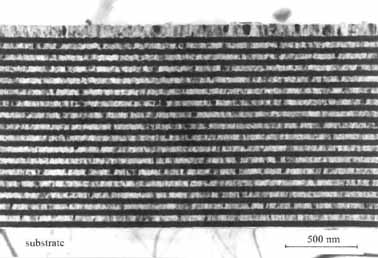
MgF2/LaF3 multilayer UV mirror (for l = 248 nm) |
|
|
Multilayers are typical examples of
artificial nanostructured materials. They often called supperlattices due to
their one-dimensional periodicity. Due to small dimensions of the layers
(1-100 nm), multilayers have unique properties compared to their bulk counterparts,
which opens the way to applications. In hard coatings, the interfaces hinder
dislocation motion making the hard coatings even harder. Electromagnetic
waves can be reflected at the interfaces providing the operation principle
for interference mirrors in UV and X-ray wavelength range. For technological
purposes deposition of multilayers with uniform layers and abrupt interfaces
is necessary. In many cases the multilayers are deposited at low temperature
(below 1/3rd of the melting temperature) where columnar growth can occur
making the interfaces wavy. The columnar structure is an intrinsic property
of the multilayers: its development is a consequence of the nucleation and
coalescence, which occurs at each interface. On the contrary, nodular growth
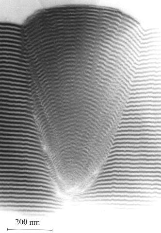
originates from irregularities of the substrate surface. In the figure below
(left) simultaneous appearance of nodular growth and columnar structure can
be seen. Though their origin is different, their further development is
supported by the same growth phenomena, e.g. shadowing and low surface
mobility of adatoms. Surface mobility can be enhanced by energetic surface
bombardment, but it can decrease the abruptness of the interfaces. |
|
|
A parabolic defect (node) in an amorphous Si/Ge multilayer. The node emerged from a local irregularity of the substrate. Note the columns both in the node and around it. |
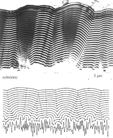
Growth morphology of a Si/Ge multilayer grown on an artificially rough substrate. The figure below is the simulated growth front calculated by the Huygens principle (from C. Tang et al. Phys. Rev. Lett. 64 (1990) 772). |