|
|
|
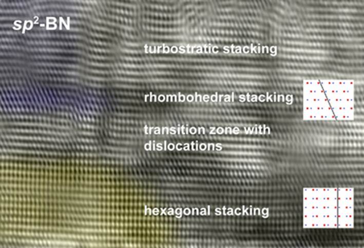
Cross sectional HRTEM image of sp2-BN grown on 6H-SiC. After a thickness of 4 nm, the h-BN growth
is followed by r-BN growth as
a result of stress relaxation. |
|
Boron nitride
(BN) is a promising semiconductor
material for application as microelectronic components such as optoelectronic,
radiation detection, spintronic, biosensing, high-temperature, and radiation
resistant devices. Boron nitride (BN) is a wide band gap semiconductor
with a direct band gap of around
6 eV, high thermal and chemical stability, high thermal conductivity, and a low density. BN can exist in sp2- or sp3-hybridized form
where the former possesses two crystal structures:
hexagonal (h-BN) and rhombohedral (r-BN). The epitaxial BN films were deposited at Linköping University
in a hot-wall CVD reactor at 1500ºC using triethyl boron (TEB, B(C2H5)3) and ammonia (NH3) as
boron and nitrogen precursors
and hydrogen as a carrier gas. We compared the
growth of sp2-BN by
chemical vapor deposition on (0001) 6H-SiC and
on (0001) α-Al2O3 substrates
with an AlN buffer layer. Polytype-pure rhombohedral BN (r-BN) with a thickness of 200 nm is observed
on SiC whereas hexagonal BN (h-BN) nucleates and grows on the
AlN buffer layer. For the
latter case after a thickness of 4 nm, the h-BN growth
is followed by r-BN growth (see figure). We found that
the polytype of the sp2-BN films is determined by the ordering of Si−C or Al−N atomic pairs in the
underlying crystalline structure (SiC or AlN). In
the latter case the change
from h-BN to r-BN is triggered
by stress relaxation. |